©2021 Reporters Post24. All Rights Reserved.
Apple and Intel will be the first to adopt Taiwan Semiconductor Manufacturing Co.’s (TSMC) N3 (3nm) fabrication process when the contract maker of chips deploys in late 2022, Nikkei Asia news agency reported on Friday. Intel is projected to use the technology to make CPUs for PCs and servers, whereas Apple is expected to use the node for its system-on-chips aimed at client devices.
Apple and Intel are currently ‘testing their chip designs’ produced using TSMC’s N3 process, according to a Nikkei report that cites several people with knowledge of the matter. Given that N3 is about to ‘officially’ enter risk production mode in the coming weeks and assuming that the information from the news agency is correct, we can speculate that Apple and Intel have already finalized their N3 CPUs and SoCs. Though it is unclear whether they have functional silicon. Commercial production of these chips is set to start in the second half of 2022.
Intel is said to be preparing at least two products made using TSMC’s N3 node: one aimed at notebooks, another for servers. There are no details about these processors at present, but Intel has already accidentally confirmed TSMC-made Xeon SoCs aimed at various niche markets. Intel confirmed months ago that it is working with TSMC on its 2023 products, but refrained from revealing any details.
Earlier this year Intel promised that its codenamed Meteor Lake and Granite Rapids processors for client PCs and high-end servers set to be made using its own 7 nm fabrication technology were due to be launched in 2023.


The report also says that Apple is set to use its N3 SoC for its iPad tablets due in late 2022 or early 2023. Keeping in mind that Apple’s latest iPad Pros use the same SoCs as the company’s entry-level and midrange Macs, there is the possibility that the initial N3 SoC might also find its way into PCs. Subsequent N3-based devices from Apple will be used for smartphones. Apple did not comment on the story.
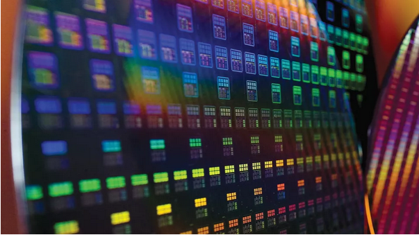
TSMC’s N3 manufacturing process is the company’s all-new node that will provide a full node PPA (performance, power, area) improvement over N5. The foundry promises a 10% to 15% performance gain (at the same power and transistor count), up to 30% power reduction (at the same clocks and complexity), up to 70% logic density gain, and an up to 20% SRAM density gain. N3 will aggressively use extreme ultraviolet lithography (EUVL) for ‘over 20 layers,’ ASML once said.
At its recent technology symposium TSMC confirmed that N3 is designed to support both smartphones and high-performance computing (HPC) applications from the very start, so the company will offer both high-performance and high-density libraries with the node. Such libraries will enable companies like Intel to maximize performance of its CPUs, whereas SoC designers will be able to pack more features into their products.
Source: tomshardware.com